
研究背景
透明电极(TEs)构成了一类特殊的材料,既具有光学透明度又具有导电性。透明电极是许多现代设备的重要组成部分,包括太阳能电池、有机发光二极管(OLED) 、液晶显示器(LCD) 、透明加热器(THs)或智能窗。传统上,透明导电氧化物(TCOs)在TEs领域占主导地位。早在20世纪50年代,宽带隙半导体(如SnO2和In2O3)的引入具有很高的光学透明度(>80%),并有可能通过杂质掺杂来提高其导电性,从而开辟了许多实际应用。因此,在实验室和工业规模上,与TCOs相关的整个生态系统和技术已经发展起来。经过60多年的广泛研究,呈现出优异光学和电子特性的氧化铟锡(ITO)薄膜现在是最常用的TE材料,它们可以通过成熟的真空溅射技术获得。然而,ITO面临着某些与它的陶瓷性质和铟的稀缺性有关的问题,这使得它不适合于某些应用,包括柔性设备。因此,ITO在太阳能电池生产中的主导地位越来越受到在寻找新材料方面取得的巨大进展的挑战,这些新材料具有更高的性能和额外的特性,如更好的灵活性、稳定性、原材料的丰富性/可用性和更低的加工成本。TCO的TE替代品包括三大类材料,也被称为新兴的透明导电材料:1)碳纳米材料,如碳纳米管(CNT)或石墨烯,2)导电聚合物,如聚3,4亚乙基二氧噻吩、聚苯乙烯磺酸盐(PEDOT:PSS)和3)金属纳米结构,如金属薄膜、金属纳米线或纤维网络或金属网格。这些纳米材料已被广泛研究,并已证明它们在解决ITO的关键问题上具有很大潜力。在这些不同的选择中,金属基的TEs似乎是最有希望的候选者,因为1)其固有的高导电性,2)通过使用纳米结构实现高光学透明度的潜力,以及3有很大的可能性有额外的能力来增加特性,如像灵活性、可拉伸性、可调带隙排列,或与其他材料结合时的适配性。
在本文中,作者总结了金属TEs的研究现状,包括金属薄膜、金属网格、金属纳米线,以及其他一些新兴的纳米结构网络,如基于裂纹模板的金属网、金属纳米通道网络、金属纤维或基于金属纳米线的纳米复合材料。对于每一种类型的金属TE,回顾了它们的主要特性、优点、缺点和制造的可行性,并将它们与TCO或其他TE进行比较。然后,讨论了在有效集成和长期稳定性方面的挑战,以便这些替代品能够获得成熟。最后回顾了在各种应用中使用金属TEs的最新进展,包括大众和利基市场。这项工作将着重于不同金属TEs解决方案之间的比较,以及未来的战略。
成果简介
透明电极(TEs) 是许多现代设备的关键部件,如太阳能电池、发光二极管、 触摸屏、可穿戴电子设备、智能窗和透明加热器。最近,对透明导电材料的灵活性和低成本的高要求需要一类新的透明导电材料(TCMs),作为传统氧化铟锡(ITO)的替代品。到目前为止,ITO一直是使用最多的TCM,尽管它很脆而且成本很高。在不同的新兴ITO替代材料中,金属纳米材料因其卓越的光电性能、低成本、易于制造、灵活性和广泛的适用性而受到广泛关注。这些材料涉及金属网格、薄的氧化物/金属/氧化物多层、金属纳米线渗入网络或基于金属纳米结构的纳米复合材料。在这篇综述中,菲尼卡大学Viet Huong Nguyen教授等人讨论了基于金属纳米材料的TCM和其他TCM技术之间的比较。接下来,介绍了迄今为止开发的不同类型的金属基TCM和所使用的制造技术。然后,讨论了这些TCM在集成到功能器件中所面临的挑战。最后,总结了金属基TCM已经成功应用的各个领域,以及新兴和潜在的应用。相关研究以“Advances in Flexible Metallic Transparent Electrodes”为题发表在Small期刊上。
图文导读
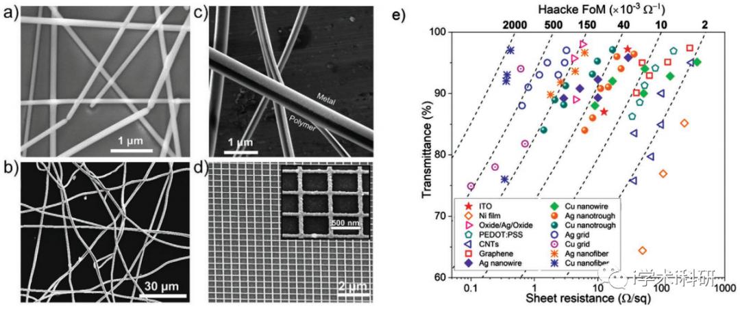
Figure 1. SEM micrographs of: a) Ag nanowire (AgNW) network with an average diameter of 60 nm.b) Cu nanofiber network on PDMS deposited by electrospinning. c) PVP polymer nanofibers coated with a thin layer of gold for the fabrication of a gold nanotrough network. d) A metal grid with a periodicity of 500 nm and a wire width of 55 nm. e) Optical transmittance at λ = 550 nm (without substrate contribution) versus sheet resistance diagram for various transparent electrodes.
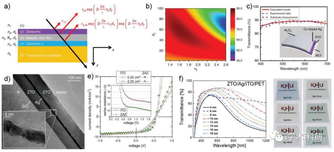
Figure 2. a) Diagram of an asymmetric OMO transparent electrode with design parameters and reflection waves at various interfaces, b) Simulated average transmittance (%) of the OMO electrode dependent on the refractive index and the thickness of the top oxide when the bottom oxide and the metallic layer are selected as 24 nm ZnO and 6.5 nm Cu doped Ag, respectively, c) calculated and measured absolute transmittance from 400 to 700 nm of the optimized 56 nm Al2O3/6.5 nm Cu–Ag alloy/24 nm ZnO transparent electrode. The transmittance (≈88.4%) of the optimized design is even higher than that of the bare PET substrate with an average transmittance of ≈88.1%. d) Cross-sectional TEM image of ZTO/Ag/ZTO multilayer transparent electrodes, and e) J–V characteristics of semitransparent organic solar cells with ITO and ZTO/Ag/ZTO top electrode for two different active areas. f) Transmittance and images of asymmetric ZnSnO(ZTO)/Ag/ITO multilayer films as a function of Ag interlayer thickness between 4 and 18 nm.
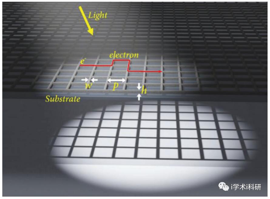
Figure 3. Diagram of a metal grid transparent electrode deposited on a transparent substrate under illumination.
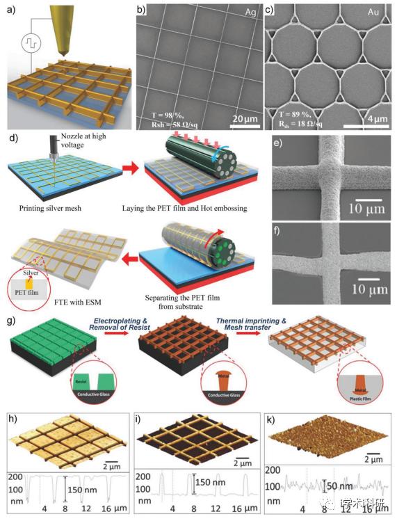
Figure 4. a) Illustration of metal grid fabrication with electrohydrodynamic NanoDrip printing. b) Printed square Ag grid with a pitch of 20 µm and an aspect ratio of 2.5. c) Truncated hexagonal Au grid with fine line-width of 80 nm, and line AR of 2.3. The values for Ag and Au samples were obtained after thermal annealing at 200 °C and 400 °C. d) A schematic of the fabrication process of flexible embedded Ag grid by electric-field-driven microscale 3D printing and hybrid hot embossing, and e,f) SEM images of the embossed- and embedded silver grids with 3 printed layers, respectively. g) Schematic illustrations of the templated electrodeposition and imprint transfer (TEIT) process: mesh patterns formed in a resist layer by lithography, electrodeposition of metal inside the resist trenches, then removal of resist to obtain standing bare metal mesh on the conductive substrate, and finally heating and pressing the metal mesh into a plastic film then peeling off the plastic film with the metal mesh transferred in a fully embedded form, and h–k) morphological characterization by AFM of embedded metal grids at different fabrication stages: PMMA nanomesh patterns by electron beam lithography, electroplated Cu nanomesh on the FTO glass substrate after removal of PMMA resist and Cu nanomesh transferred and fully embedded in a cyclic olefin copolymer (COC) film.
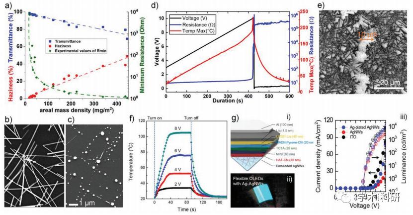
Figure 5. a) Influence of the AgNW network density on the electrical and optical properties (transparency and haze factor). b) As-deposited AgNW network. c) Spheroidized AgNW network after thermal annealing exceeding 270 °C. d) Experimental observation of the degradation of AgNW network with an initial resistance of 8.9 Ω: time evolution of resistance and maximum temperature when applying a voltage ramp of 1 V min−1, starting from 3V, until voltage breakdown observed around 10 V. e) SEM image of the AgNW network degradation or "crack" visible due to the differences in charging effect on the secondary electron detector. f) TH based on Ag NW network on PET with dimensions of 35 × 35 mm2, with a sheet resistance of 7.2 Ω sq−1 at a transmittance of 90.2%: temperature profiles upon application of different input voltages g) Flexible OLEDs with a Ag–AgNW anode: i) schematic device structure and ii) photographic image of the OLEDs, iii) current density and luminance characteristics as functions of applied voltage (J–V–L characteristics) of OLEDs based on ITO, as-coated AgNW, and Ag-AgNW anodes.
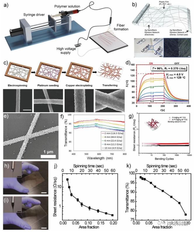
Figure 6. a) Diagram of a typical electrospinning system. b) (top) diagram of the stretchable and transparent heater composed of an AgNF network fabricated with electrospinning, and (bottom) a photograph (left, scale bar: 5 mm) and magnified optical micrograph (right, scale bar: 20 µm) of the border between the electrode and the contact pad. c,d) schematic of different fabrication steps based on electrospinning and electroplating for CuNF-based TEs and corresponding SEM image for each step: pristine PAN, platinum-seeded, Cu-electroplated, and transferred NFs. e,f) SEM image of CuNFs deposited for 6 min using the following process: electrospinning of palladium-embedded NFs, calcination to eliminate the polymer component of the NF, and Cu electroless deposition; and transmittance of CuNF-based TEs fabricated using different electroless deposition times. g) Sheet resistance of PVA@AgNF- and E-PVA@AgNF-based TEs with compressive stress at a bending radius of 2 mm. h,i) A bare CuNF-based TE and a black CuNF-based TE fabricated by normal electrospinning and coaxial electrospinning, respectively. j) Sheet resistance as a function of area fraction and electrospinning time. k) Optical transmittance as a function of area fraction and electrospinning time.
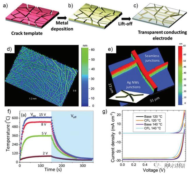
Figure 7. Schematic illustration of different fabrication steps of transparent electrodes based on the self-cracking template: a) cracked template, b) metal deposition by vacuum evaporation, c) lift-off of the template, d) the optical profiler image in a 3D view of the obtained Ag wire network. e) A closer view of a seamless-junction Au-wire network fabricated from the self-cracking template and vacuum evaporation, the image was captured from an optical profilometry. The inset image illustrates a typical junction between single crystal Ag nanowires for comparison purposes, f) temperature profiles of the Au-wire network/quartz as a function of time at different applied voltages recorded using an IR camera. g) Light and dark J–V characteristics of GaAs solar cells with front grids patterned by cracked film method and standard lithography, resulting in devices of high energy-conversion efficiencies: 26.4% and 24.7%, respectively.
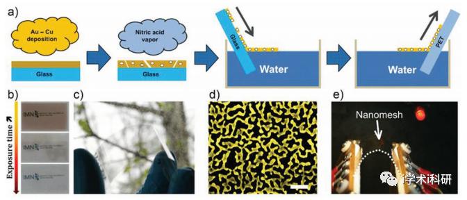
Figure 8. a) Diagram showing different steps to fabricate Au nanomesh electrodes: cosputtering of Au–Cu ultrathin film, which is then exposed to nitric acid vapor before being transferred to PET substrate. b,c) Photographs showing the evolution of an Au–Cu film versus exposure time to nitric acid vapors and a gold nanomesh on a PET substrate. d) Colorized SEM image of a 10 nm thick gold nanomesh prepared using Au–Cu film with an initial Au content of 17 at%, scale bar: 200 nm. e) Photograph of a nanomesh electrode on a flexible PET substrate under a strain of 1.2%, being used to switch on a red LED.
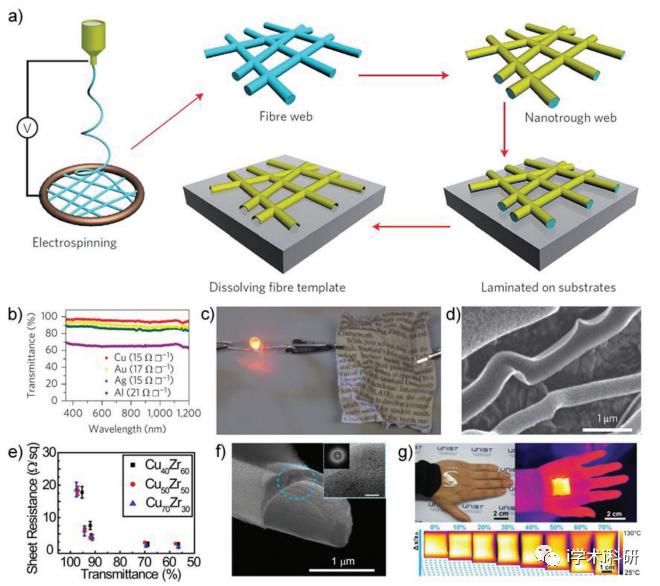
Figure 9. a) Fabrication and transfer process for metal nanotrough networks: electrospinning of polymer nanofiber templates, deposition of metal layer, transfer of coated nanofibers to a desired solid substrate, and finally dissolution of polymer–fiber templates. b) Transmittance of metal nanotrough networks made of different metals, showing excellent optical-electrical performances of the Cu/Au nanotrough networks. c) Photograph of Au nanotrough networks on paper after mechanical deformation. d) SEM micrograph of Au nanotrough networks on Al foil after folding. e) Transmittance versus sheet resistance of the CuZr nanotrough network (prepared by electrospinning and cosputtering process). f) SEM micrograph of a CuZr nanotrough, the inset TEM image with Fourier transformation diffraction pattern indicating the amorphous nature of the alloy. g) IR images of transparent heaters based on the CuZr nanotrough networks (prepared on PDMS substrates) under various tensile strains.
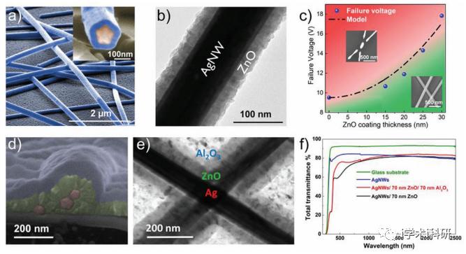
Figure 10. a) Colorized SEM image of AgNW networks coated with 30 nm ZnO (deposited with SALD) with a small back-scattered SEM image of a coated AgNW showing the usual fivefold symmetry twinning of AgNWs surrounded by a uniform 30 nm thick ZnO layer. b) TEM image of a 30 nm thick ZnO-coated AgNW. c) Failure voltage dependence versus ZnO coating thickness. d) SEM image (false-colored) of a cross-section of AgNW networks coated with 70 nm of ZnO and 70 nm of Al2O3. e) TEM image of a thick ZnO and Al2O3 coating (deposited with SALD) around two different AgNWs. f) Total transmittance spectra of a bare AgNW network and networks coated with ZnO and a combination of ZnO and Al2O3 coating of 70 nm each
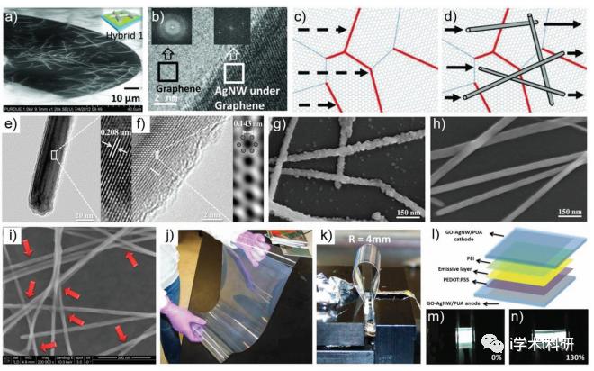
Figure 11. a) SEM image of AgNWs and graphene nanocomposite, b) TEM image of the interface between graphene and a single AgNW. c) Diagram representing the electrical transport through the grain boundaries (GBs) in single-layer graphene and d) the hybrid composite of graphene and AgNWs. e,f) HRTEM image of the CuNW–graphene core–shell nanostructure with a zoom on the CuNW part, and HRTEM image of the edge of the core–shell nanostructure, g,h) SEM images of CuNW and CuNW–graphene nanostructures, before and after the stability test, respectively. i) SEM image of soldered junctions of AgNWs assisted by the presence of graphene oxide, j,k) photographs of a graphene oxide–AgNW on PET substrate. l) Schematic illustration of a stretchable polymer light-emitting diode (PLED) using GO–AgNW composite electrodes, and m,n) a PLED of original lighting area of 3mm × 4 mm, and stretched at a strain of 130%.
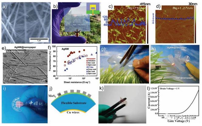
Figure 12. a) SEM micrograph and b) transparent antenna of the AgNW networks and PEDOT:PSS nanocomposite. c) AFM image of the bare AgNWs and d) AgNWs incorporated on PVA with a reduced surface roughness. e,f) SEM images of AgNW@cellulose nanopaper prepared by filtration coating and comparison of transmittance at λ=550nm as a function of sheet resistance for AgNW@cellulose nanopapers prepared by different techniques. g,h) Paper craft by using transparent conductive paper with AgNW and a light-up LED. i) Nanopaper composed of CuNWs and cellulose under bending, j–l) diagram, photograph and I–V characteristics of a thin-film MoS2 transistor as the cellulose works as dielectric layer and CuNWs as back electrodes.
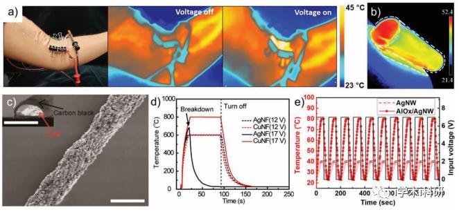
Figure 13. a) Photograph and IR images of the temperature distribution in a bioinspired thermotherapy patch to the cubital fossa area, based on AgNW TH. b) IR image of a flexible TH based on a patterned 8.4 nm thick Ag grid on ZnO-coated PE substrate, bent into a roll (6 cm × 6 cm), under 5 V bias. c,d) SEM image of black CuNFs with a cross-sectional inset image of the CuNF (scale bar: 1 µm), and demonstration of extremely high-temperature heaters using SiO2-coated AgNF and black CuNF networks. e) ON/OFF responses of AgNW-based heaters with and without AlOx coating layer.
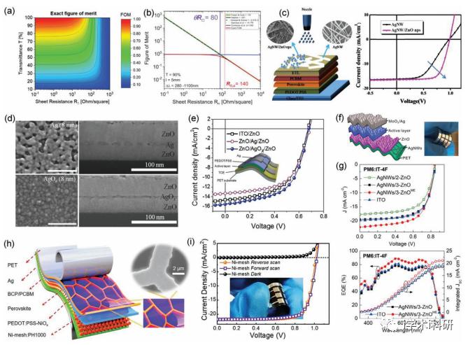
Figure 14. a,b) FoM based on the calculation with the impact of transmittance and sheet resistance on photovoltaic performance for the spectral range of [280, 1100 nm] and a solar cell length of 5 mm. c) Diagram and cell performances of solution-processed semitransparent perovskite solar cells with spray-coated AgNWs and AgNWs/ZnO composite top electrode, showing a PCE improvement from 7.31% to 11.13%. d) Top-view SEM micrographs of Ag and AgOx deposited on 50 nm thick ZnO films, and cross-sectional SEM micrographs of ZnO/Ag/ZnO and ZnO/AgOx/ZnO TEs using 8 nm thick Ag and AgOx layers, respectively. e) J−V characteristics of inverted organic solar cells (IOSCs) using different TEs. The inset represents the device architecture of flexible IOSC fabricated on a PET substrate. f) Diagram and photograph of a flexible OSC with moth-eye nanopatterned AgNWs/ZnO TEs on a PET substrate. g) J–V curves and EQE spectra of PM6:IT-4F-based OSCs. h) Diagram of the perovskite solar cells with Ni mesh/PEDOT:PSS hybrid TE and SEM micrograph of the Ni mesh. i) J–V curves of the PET/Ni mesh-based perovskite solar cells.
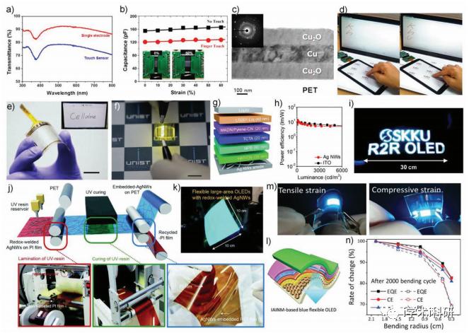
Figure 15. a) Transmittance of stretchable AgNW/reduced graphene oxide (rGO)/polyurethane (PU) electrode and stretchable capacitive touch sensor with two AgNW/rGO/PU electrodes, b) variation of capacitance in the AgNW/rGO/PU capacitive touch sensor under different strains. c,d) Cross-sectional TEM image of the Cu2O/Cu/Cu2O multilayer electrode and photographs of capacitive-type flexible touchscreen panels based on patterned Cu2O/Cu/Cu2O mesh electrodes. e,f) photograph of a touchscreen panel based on AgNWs-coated transparent cellulose nanofiber hybrid films, and a photograph of a TOLED emitting light through both directions. Reproduced with permission. Copyright 2016, Springer Nature. g–i) schematic illustration of an OLED based on a AgNW anode, power efficiency versus luminance for OLEDs based on the AgNWs and ITO, and a light-emission images of a large-area flexible OLED based on an AgNW anode, fabricated with roll-to-roll process, respectively. j,k) Schematic illustration of the roll-to-roll embedding process used for the redox-welded AgNWs, and light-emission image of large-area flexible OLEDs under bending. l) schematic structure of an IZO/Ag/IZO nanomesh-based blue flexible OLED, also called IAINM OLED, m) photographs of the IAINM OLED under tensile and compressive strains, n) experimentally measured external quantum efficiency (EQE), current efficiency (CE), and power efficiency (PE) of IAINM-OLED (bold) and AgNM-OLED (open) after 2000 times bending cycle at a bending radius of 2.0–0.3 cm.
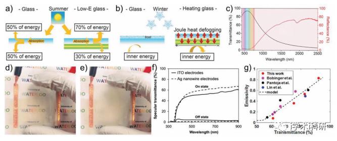
Figure 16. Applications of metal-based TEs related to energy saving. a–c) Schematic diagrams comparing: a) the thermal insulation effect of AZO/ Ag/AZO based low-emissivity glass and untreated glass in hot weather and b) the defogging effect of AZO/Ag/AZO-based low-emissivity glass in cool weather. c) Transmission and reflectance spectra of an AZO/Ag/AZO-based low-emissivity heater. d–f) Integration of a AgNW network as a TE in a polymer-dispersed liquid-crystal (PDLC) based smart window: d) images obtained with 85 V (on state, associated to an electric-field of 3.4 MV m−1 and e) without voltage (off state) applied across opposite electrodes. f) Specular transmittance of the AgNW network and ITO used as TEs in a PDLC smart window in the on and off states. g) Dependency of emissivity in the infrared spectra (5–20 µm) versus optical transmittance (550 nm) of silver nanowire networks. For low-emissivity applications, the search area is low-emissivity and high optical transmittance, i.e., in the bottom right area of the graph.
总结展望
金属TEs的主要优势之一是其制造工艺,例如,喷涂、槽模、棒状涂层和印刷技术,通常不需要真空室或高温处理。相反,用于主要金属TEs的溶液工艺可以很容易地扩展并与卷对卷技术兼容;因此它们可以是低成本和环保的。金属TEs有关的未来道路无疑与纳米复合材料的制造、优化和使用有关,其中金属可以与其他材料(如聚合物、碳基材料或氧化物)混合。即使是一层薄薄的氧化层也能极大地提高AgNW网络的电和热稳定性。这对基于CuNW的TEs来说也是一个明显的优势,其稳定性在涂上一层薄薄的氧化层后也会增强。这是相当有希望的,因为铜基材料的成本比银低得多,尽管由于铜容易被氧化,它们确实给集成带来了某些挑战。已经探索了几种涂层方法。其中,一种新兴的、有前途的方法是大气压空间原子层沉积(AP-SALD) ,它可以在相当低的温度下沉积保形的薄的氧化物涂层,并且由于其成本效益和与大型升级方法(如卷对卷)的兼容性,应该在未来发挥重要作用。所获得的涂有薄而保形氧化层的MNWs构成了灵活而稳定的透明电极,而且还可以显示出更好的物理特性,因为薄的氧化层也可以作为抗反射涂层。
金属TEs的前景还涉及到相关的开发和/或使用表征技术,以更好地研究适当规模的材料特性。由于大多数金属TE技术是不均匀的(除了电介质-金属-电介质技术),能够在最适当的尺度上进行测绘是非常重要的。另一方面,对更好地理解和优化金属TEs的一个重要贡献应来自于它们的建模。建模可以帮助更好地理解主要参数(如化学成分、制造方法和条件、几何方面和沉积后处理)对其物理特性的影响。这不仅对了解金属TEs中使用的功能材料的行为至关重要,而且对详细调查在其集成中起关键作用的相关界面也至关重要。例如,缺乏粘性将是非常不利的。建模通常是基于真实功能材料层的物理方法,所获得的主要结果可以有效地作为输入,并指导更好地设计金属TEs。
最后,金属TEs可以构成许多应用领域中工业发展的关键部件。诸如金属纳米线或金属网等技术已经出现在市场上,用于潜在的大规模应用。然而,它们在商业产品中的整合还没有得到广泛的应用。由于目前对金属基技术的深入研究,我们应该在未来几年见证这一领域的许多 创新,要么与新的金属基技术有关(如通过使用不同的材料),要么与当前技术尚未覆盖的新应用领域有关。由于金属TEs的低成本和吸引人的特性,在不久的将来,可以在柔性光伏、可折叠设备、可穿戴电子设备、节能设备或软机器人等领域发挥主导作用。
文献链接
Advances in Flexible Metallic Transparent Electrodes, Small 2022, 2106006, DOI: 10.1002/smll.202106006.
https://doi.org/10.1002/smll.202106006.
厦门柔性电子研究院
福建省协同创新院柔性电子产业技术分院
地址:厦门市集美区集美大道1995号科技成果转化加速器1期4F
邮编:361024 电话:0592-5366222 邮箱:admin@flex-elec.com
部分图片来源于网络,如有侵权请联系删除