

研究背景
随着对便携式、轻量级和低成本的柔性和可穿戴电子产品的需求不断增加,大量研究关注解决下一代电子设备构造方面的未来挑战。此外,之前报道的数据显示,器件的灵活性经历了从平面器件到柔性(2013年)和可拉伸(2018年)器件的广泛进展,目前和未来的重点是可折叠和可变形(2021年)器件。对可穿戴和可植入设备的需求有效地推动了柔性电子材料市场的发展。目前,研究的重点是构建高度灵活、柔软、无刺激和无毒的特性,此外还有成本效益。要实现上述在可变灵活性、作用机制和利用模式方面的多种特性,需要对柔性基底进行大量研究。柔性基底在导入若干特性以实现各种特性方面起着关键作用,如用户的舒适性、灵活性以及时尚设计和小型化的能力。一般来说,柔性可穿戴系统中的设备基础设施包括三个主要组成部分:导电网络、基底和功能材料层。在这些组成部分中,基材控制着整个设备的特性,而这些特性取决于材料的组成。因此,为了实现卓越的机械坚固性、高电子性能以及柔性和可穿戴设备所需的关键特性,有必要选择和整合具有合适特征的基材技术。这些特征可能包括机械灵活性、润湿性、渗透性、生物相容性、生物吸收性、耐热稳定性、表面光滑性、低厚度、低成本和光学透明性。且为了使一个系统具有伸展性和机械灵活性,不同的设计策略和工程方法对于设备结构及其排列的修改同样至关重要。
成果简介
深圳大学徐秀茹、彭争春等人概述了柔性和可穿戴系统的进展,重点介绍了整合灵活性和稳定性的关键柔性基材,以实现柔性电子设备的构建和运行。作者从柔性电子设备中基材选择所需的化学、热、机械、附着力和生物相容性等方面提供了一个全面的介绍。此外,还进行了简要的讨论,以强调在柔性和可穿戴设备方面,柔性基材的设计、组装、制造和应用策略的最新成果。这是为了验证使用柔性基材作为最有效的平台之一,在高压缩、拉伸或扭曲的条件下提供优秀的粘附特性和设备稳定性;从而在各种潜在的应用中产生卓越的性能和更高的可控性。最后,讨论了柔性基底的未来挑战和前景。
图文导读
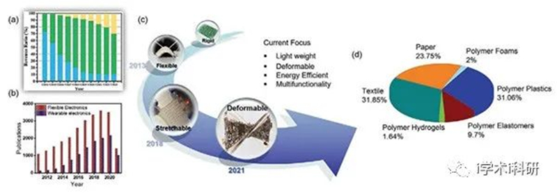
Figure 1. a) Global revenue ratio of stretchable, flexible, and rigid electronics. b) The number of publications for the last 10 years for ‘‘wearable electronics’’ and ‘‘flexible electronics.’’ c) Graphical presentation for the development in the flexibility of devices. d) Relative distribution of a number of the paper published for last 10 years for different polymer substrates including polymer plastics substrates with the keyword, (PET substrate, PI substrate, PEN substrate, and PC substrate) and polymer elastomer substrates with keywords (PDMS substrate, PU substrate, TPU substrate, SEBS substrate. Other substrates including polymer hydrogels, polymer foams, textile substrate, and paper substrates data are also indexed in the Web of Science in June 2021.
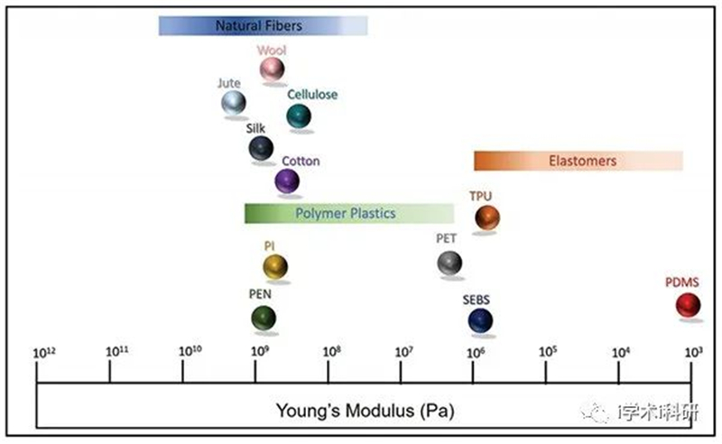
Figure 2. Young’s modulus (unit: Pa) of widely used materials for flexible and wearable systems.
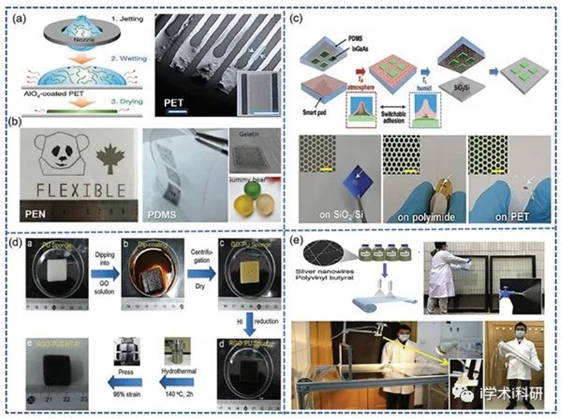
Figure 3. a) Schematic of inkjet printing for MXene with ultrahigh-resolution and its SEM image. b) Image for inkjet printing of AgNPs on flexible PEN substrate with Photograph of printed carbon MEAs on a PDMS, gummy bear, and gelatin substrate. Reproduced with permission. c) Smart printing schematic of InGaAs (square-patterned) onto SiO2/Si substrates including InGaAs nanomembranes transfer using the smart adhensive pad, consists upon the high and low-adhesion state. An optical and microscope picture of a hexagonally patterned Si membrane is shown at the bottom. SiO2/Si, PI film, and thin PET substrates were sequentially transferred (from left). Reproduced with permission. d) Schematic of synthesis as well as pressure-sensing models of graphene-wrapped PU sponges, RGO–PU, RGO–PU–HT, RGO–PU–HT–P sponges and their SEM images (right side). Reproduced with permission.[90] Copyright 2019, Wiley-VCH. e) Diagram for R2R spray coating of Ag NWs/polyvinylbutyral on PET substrate. Reproduced with permission.
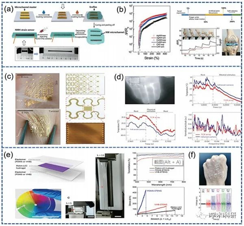
Figure 4. a) Schematic diagram for fabrication of NMH sensors. b) Photograph of under stretched and relax state and its application for the movement detection of skeleton knee model (black), and the tensile strength under different deformations (red). Reproduced with the permission.[146] Copyright 2018, Springer Nature. c,d) Optical and magnified image (single sensor) of 4 × 4 temperature coefficient of resistance integrated on a thin elastomeric substrate and applied on the skin by using water-soluble adhesive. IR image is for palm mounted sensor during stimulus experiments. Infrared camera output graphs represent the temperature of the palm (blue) and a sensor array (red) during mental. Reproduced with permission. e,f) Schematic diagram of sandwich structured TENG and its optical image during the stretched state, attached on hand with 3 × 3 pixels. Graphs illustrate the voltage profiles at 5 different pressures. Reproduced with permission.
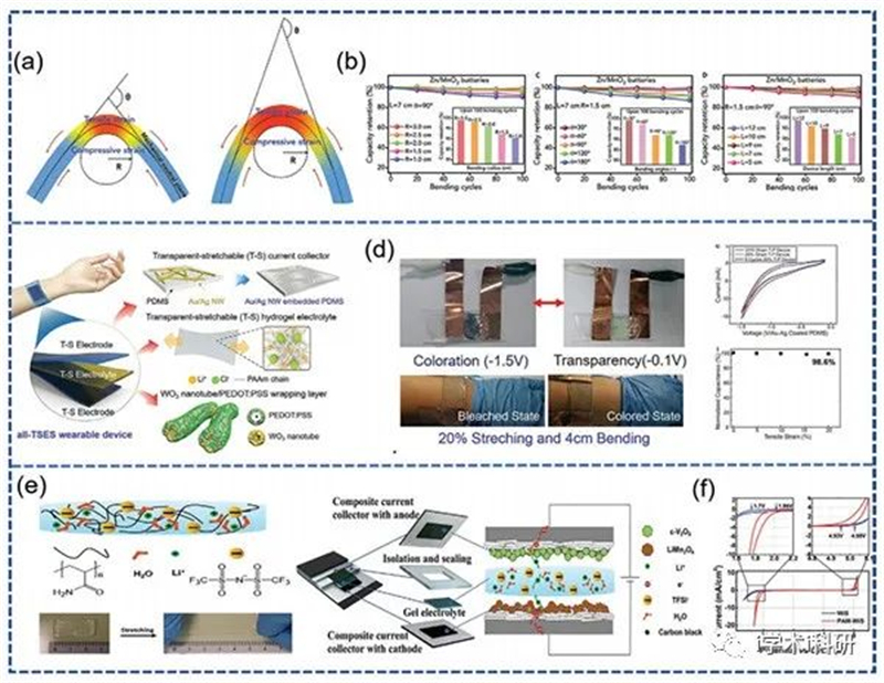
Figure 5. a,b) Key parameters (L, q, and R), used for bending state of flexible and wearable energy storage devices. Reproduced with permission. c,d) Schematic diagram of stretchable and transparent electrochromic supercapacitor. Au/Ag core–shell with acute oxidation resistance, flexible and stretchable hydrogel electrolyte, WO3 nanotube, and wrapping a layer of PEDOT:PSS. Illustration of the arm-wrapped all-TSES device with 20% stress in cyclic voltammetry and variation in capacitance. Reproduced with permission. e) Schematic illustration with photographs of the unstretched and stretched PAM/WIS gel. f) Schematic figure of stretchable full cell.
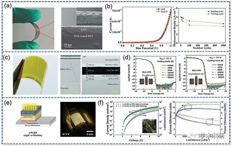
Figure 6. a) Photograph of GDY-based photodetector with SEM images. b) Photo-response of GDY-based photodetector with the mechanical response (bending and twisting cycle). Reproduced with permission. c) Optical image of the flexible thin-film transistor (TFT) on PI substrate with corresponding SEM image. d) TFT performances comparison of BLA poly-Si TFT measured parallel and perpendicular to the current path after folding until 30 000 cycles. Reproduced with permission. e) Device architectures and photographs of a-PLED arrays with fine lines on glass and PEN substrates. f) Working efficiencies of a-PLEDs on PEN substrates.
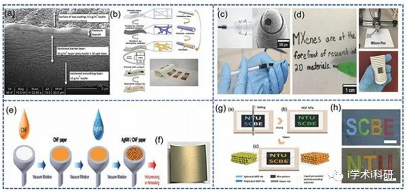
Figure 7. a) Focused ion beam etched cross-section image. Reproduced with permission. b) Schematic diagram of flexible RFID tags on paper substrates by surface modification, inkjet printing, and electroless deposition, respectively. c) Optical image of rollerball pen representing direct writing of Ti3C2 inks. d) Water dissolved Ti3C2 for paper writing with computer-controlled drawing apparatus (AxiDraw) and versatile patterning of AxiDraw at the right side. e) Schematic of step by step fabrication for Ag NWs/CNF paper by vacuum filtration method. f) An optical image of Cellulose-based TENG. g) Precise illustration for Mayer rod coating of MOF APS patterns with h) selective wetting (hydrophilic area of the substrate), ii) formation of APS patterns (after water removal), iii) vapor-responsive color changes by spherical/polyhedral MOF inks, and multicolored photographs of letters respectively.
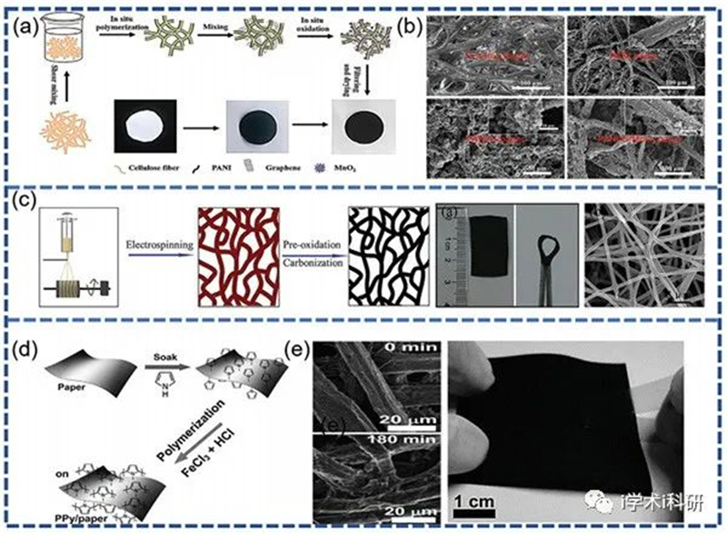
Figure 8. a) Schematic procedure, exhibiting the polymerization of PANI on printing paper to form PANI/G/MnO2 hybrid. b) SEM images of Printing paper, PANI paper, PANI/G paper, and PANI/G/MnO2 paper, respectively. Reproduced with permission. c) Schematic for the fabrication process of cross-linked carbon nanofibers. Right side optical image of the cross-linked N-doped carbon nanofiber network before and under folding. d) Schematic diagram of the fabrication of polypyrrole-coated paper. e) SEM images for polypyrrole-coated paper at 0 and 180 min after polymerization. Tape test showing very strong mechanical property of the final prepared polypyrrole-coated paper.
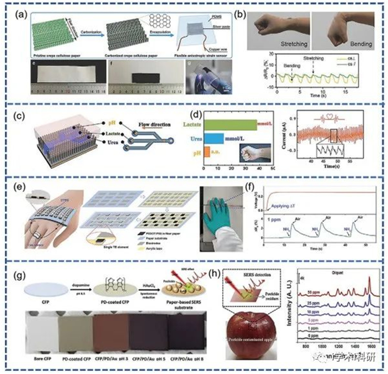
Figure 9. a) Schematic diagram for the fabrication mechanism of the flexible carbonized crepe paper (CCP) strain sensor. Photograph at lower side representing the carbonization of CCP before and after the treatment. The final image is in working condition of the flexible CCP strain sensor. b) Working of CCP sensor during stretching and bending of the wrist. The graph shows the resistance change during stretching–bending of the wrist. c) Schematic representation of artificial skin based on integrated microfluidic and nanogenerator for simultaneous monitoring of sweat and pulse during running. d) Detection of lactate and urea concentrations during running by artificial skin. Graphical representation of current changes in artificial skin during pulse sensing and the inset shows the image of artificial skin attached to a human wrist. e) Schematic diagram for the fabrication mechanism of OTE generator with PEDOT:PSS legs. Working photograph of an OTE array powered chemical sensor attached on hand. f) Optical image of an OTE array powered chemical sensor attached on the middle finger. The right side graph represents the monitoring of voltage output caused by a temperature difference between a heating plate and a cooling flow. g) Schematic diagram of synthesis mechanism for paper-based SERS substrate. Surface morphology and optical property observations of bare cellulose filter paper (CFP), PD-coated CFP, and SERS substrates from left to right at different pH values. h) Schematic illustration of pesticide observation with a paper-based SERS substrate on an apple surface. Graphical representation of Raman spectra of DQ with pesticides at various concentrations.
Figure 10. a) Schematic diagram for the synthesis process of i) Ti3C2Tx MXene, ii) RuO2·xH2O@MXene nanocomposite, and iii) flexible MSC devices. b) Electrochemical response of R@M-A0.75:1 micro-supercapacitors:galvanostatic charge/discharge profiles from 0.1 to 0.6 mA cm−2 (four different current densities). The graph at the bottom represents capacitance change during multiple bending cycles under the constant strain of 5.0% (inset: contrastive CV curves recorded at 100 mV s−1 before and after 2000 bending cycles). c) Schematic diagram consisting of optical images of MLP synthesis. d) Graphs represent the charge–discharge curves (in 0.01–2.0 V at 20 mA g−1 ) and cycling response of MLP at multiple mass loading (in 0.2–1.0 V at 0.5 A g−1 ) at top and bottom, respectively. e) Optical images of mechanical test for MLP showing complete recovery after bending cycle. f) Structural diagram of PTENG and its triboelectric response under constant stress (at a frequency of 10 Hz) in the form of load voltage output and short-circuit current output (Isc), respectively. g) Circuit diagram of P-TENG attached in the bridge rectifier. Optical image of P-TENG during the lightening of multiple green and blue LEDs under repeatedly pressure stress (9.6 kPa at a frequency of 10 Hz). Graphical verification of P-TENG self-powered touch sensing. h) Structural diagram of the paper-based solar cell. Optical images of final devices with PEDOT: PSS and Ag contacts i) P3HT: PCBM, and ii) PTB7:PCBM devices from left to right, respectively. i) Box plot diagram of normalized median value i) P3HT:PCBM and ii) PTB7:PCBM at different area paper devices.
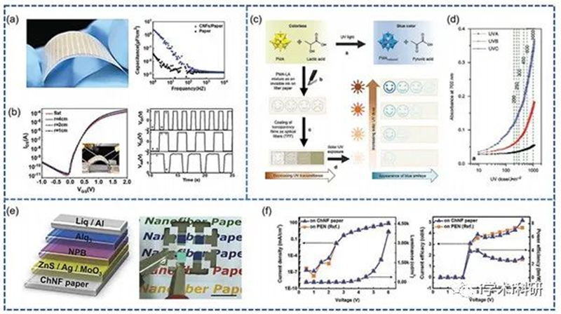
Figure 11. a) Optical image of the flexible TFTs and capacitance changes under different frequencies of CNFs-soaked and the regular paper. b) TFTs responsive curve at different bending radii with an optical image of the bent device during measurements (inset). Logical measurement demonstration of NAND logics in flexible TFT. c) Schematic for synthesis mechanism of paper-based colorimetric UV sensor. d) PMA–LA response for UVR dose showing its ability to make difference between UVA, B, and C. Three plots represents responses for UVB MED (200, 250, 300, 450, 600, and 1000 J m−2 , respectively). e) Structural diagram of OLED and optical image of flexible OLED build on ChNF paper. Working of OLEED in flat and flexed state on the left and right side at 1 cm scale bar. f) Graphical representation of OLED’s J–L–V characteristics, fabricated on a ChNF paper for analysis and a PEN film for reference.
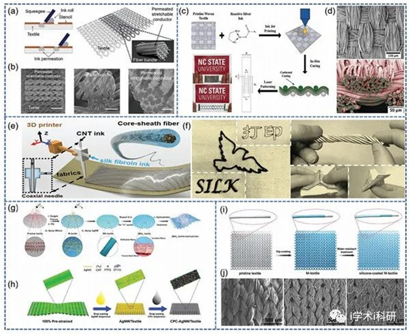
Figure 12. a) Schematic of direct stencil printing on textile and illustration of permeated composite in a single fiber bundle. b) Surface and cross-section SEM images of printed wiring and textile before and after printing, respectively. c) Schematic diagram for synthesis and characterization of laser cutting printed e-textiles. d) Surface SEM of pristine woven at 150 μm and cross-sectional SEM image of a printed woven indicating red (silver coating) on grey (individual fibers). e) Schematic elaboration of 3D printing mechanism utilizing the coaxial spinneret. f) Images of patterns designed on textile, English word SILK, flying pigeon, and Chinese characters. Twisted and folded images showing flexible behavior of smart textile. g) Schematic diagram indicating manufacturing process of conductive, hydrophobic, and permeable silk textile by layer-by-layer fabrication approach. h) Schematic for deposition of Ag NWs and CPC to form CPC-AgNW textile. i) Schematic of manufacturing PPy/MXene-decorated and silicone-coated PET and M-textile respectively. j) SEM images of pristine, M-textile, and silicone-coated M-textile (from left to right).
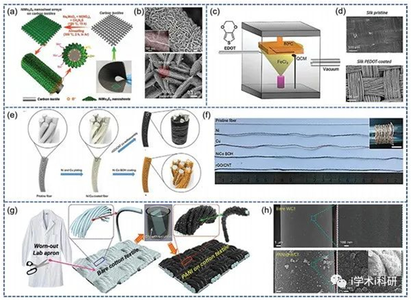
Figure 13. a) Schematic diagram of fabricating 3D hierarchical nanosheet (NiMo3S4) patterns on carbon textiles. b) SEM images of NiMo3S4/CTs at different magnifications. c) Structural diagram of the vapor deposition system. d) SEM images of pristine silk textile and PEDOT-coated silk textile. e) Schematic of the manufacturing mechanism of Y-ASC. f) Optical image of yarns for multiple coatings (Ni, Cu, Ni-Co BOH, rGO/CNT). g) Schematic illustration for PANI deposition on WCT surface. h) High-magnification SEM results of pristine and PANI coated onto the WCTs.
总结展望
与刚性电子器件相比,柔性电子器件除了具有不同的灵活性、低质量、便携性和机械强度等优点外,还表现出更优越的性能和更实用的实施。在柔性电子中,除了赋予一定程度的灵活性外,柔性基材在提供机械灵活性、低质量、低厚度、机械强度和低成本方面发挥着关键作用。本综述着重强调阐述了柔性基底对于制造柔性和体网系统的意义,它是构建从基本电子元件到集成平台的低成本、高效电子器件的基础。基于这种技术,许多应用可以实现,并具有明显的优势。然而,有几个限制需要克服,如下所述。1)选择具有合适的热、化学、电、机械和形态(表面)特性的基底;这也是实现用户舒适性、灵活性、时尚性和小型化等不同特性的要求。一个理想的基材应该在加工过程中表现出热和化学稳定性。此外,为了在实际应用中实现灵活的设备,高机械灵活性和优秀的粘附性能是可取的。2)对于衬底加工,根据衬底的行为,选择具有简单操作和成本效益特点的合适的制造技术是关键。鉴于基材的热稳定性会诱发尺寸稳定性,最佳的条件,如操作温度应与所需基材的热特性相匹配。因此,低温物理方法,如印刷和涂层方法更适合于柔性基材的加工。然而,由物理方法导致的基材和沉积材料之间的接触不良可能会导致性能下降。因此,几种反应条件温和的化学方法已被广泛用于特定的基材,如织物基材和碳纸基材,从而为更复杂的结构提供大面积的沉积,并具有良好的表面接触。3)在基底的功能修饰过程中,纳米材料的可用性对物理特性,如分辨率、结构精度和功能有很大影响。因此,开发具有增强性能的先进材料对于在各种基材上实现柔性电子器件的新功能特性是可取的。4)对于柔性和可穿戴设备的制造,除了防止电极断裂和性能下降外,设备的制造设计对于机械变形下的高稳定性至关重要。其他因素可以作为进一步研究的基础,例如,完全小型化的结构、便携性和出色的身体网络系统。5)对柔性和可穿戴设计的全面评估是以用户为中心,并考虑所有潜在的商业机会。应考虑指标体系开发过程的系统性、层次性和全面性,为柔性/可穿戴产品设计建立科学、公正的指标体系评价。三个标准构成了对柔性/可穿戴设备设计的评估要求。首先是"用户要求" ,即柔性设备应至少满足一个严格的标准,以确保和改善人类的福祉。对于用户要求,五个用户的影响标准被认为是必要的,如时间、质量、服务、设计和感知价值;每个标准都有一个独特的分数,以评估可穿戴和时尚商品能够满足用户要求的程度。第二部分是"用户场景”,提出了一个案例,即可穿戴智能设备在很长-段时间内被频繁使用,而且是以不可替代的方式。产品的开发应符合多元回归和评估程序的结果,包括频率、长度和不可替代性的不同影响因素。同样,第三个组成部分是"用户体验",它包括美学和情感体验,同时决定是否购买产品。因此,这三个组成部分与最初的设计目标有关,并评估了柔性何穿戴设备的关联。产品设计的功效和可靠性提高了产品的性能,从而使其能够满足需求方案的三个标准。6)此外,柔性设备的环境风险和危害是关键的关注点。由于电子设备的快速升级,一些设备被丢弃,从而导致了危险的环境污染,增加了环境威胁。由于聚合物基材的低成本、低质量和耐用性,它们被广泛用于电子设备中,应用范围广泛。然而,由于塑料基材在土壤和自然栖息地中的低降解性,生产能力的显著增加诱发了关于废弃的报废塑料设备的问题。为了减少这些环境威胁,需要建造由可再生和可生物降解的基材以及少量潜在有毒材料组成的电子系统。此外,纤维素基纸和纺织品基底为可生物降解的数字电子产品提供了一个平台,在可生物降解的柔性纤维素基纳米纤维纸和纺织品基底上消耗少量的潜在有毒材料,这明确证实了使用生态友好材料制造高性能柔性电子设备的可行性。7)电子废物的迅速增加威胁着地球上的生命,并对环境造成不可逆转的破坏。因此,有必要减轻不可降解的电子设备的重大影响,并为子孙后代再生环境。科学家和专业人士考虑的一个有效方法涉及电子设备的回收,因为替代方法如高温燃烧是不可取的,因为会产生有毒气体(如二氧化碳和残留物),对环境有害。在维持环境方面,回收需要较少的能源来生产原材料,并将对原材料的要求降到最低,从而有助于保护自然资源。回收过程表明,在收集、清洗、分类和减少废料尺寸的基础上,回收率有了大幅度的提高;从而证实了消除环境污染废料的实际意义。8)此外,植入式智能电子设备将在不久的将来引发护理点保健和人机界面领域的革命。随着无线充电技术和灵活的纳米发电机的不断进步,这些长期稳定和自我供电的植入式生物医学系统将成为重要的现代临床诊断和治疗工具。其中,新型材料的开发和与柔性基底集成的器件配置将是植入式智能电子领域最关键的技术。然而,目前用于植入式电子器件的柔性基底的兼容性还远远不够理想,缺乏完美粘附和符合人体组织或器官形状的能力,没有表现出良好的生物吸收性,不需要在以后的手术中移除电子器件,也没有抗菌和抗炎的特性等。这一领域的未来工作可能集中在开发灵活的、具有生物功能的基质,这些基质由新型天然和合成聚合物以及具有平面、织物甚至纺织品结构的聚合物复合材料制成,与能量生成和存储系统相结合,以智能监测和控制体内的植入式医疗设备。基于上述讨论,它概述了柔性基底在柔性和可植入系统中的新兴应用,同时回顾了三种不同类型的柔性基底,即聚合物基底、纸基底和纺织基底。这些柔性基底赋予了许多特性,如润湿性、密度、机械灵活性、耐热性和表面光滑度、低厚度、低成本,甚至透明的柔性电子器件。此外,在不久的将来,柔性电子设备的功能集成的发展将实现商业化。为了将实验室研究的规模扩大到商业水平,需要进行大量的研究,以生产具有成本效益和坚固的自然设备,用于实际商业应用。因此,需要进一步的研究来选择合适的基底,以实现各种参数下的理想特性,如热稳定性、化学稳定性、机械灵活性、表面光滑度和附着力。此外,基底上的功能处理需要合适的制造技术以确保柔性电子应用的可行性。因此,研究界和工业界之间的合作是必要的,以便更好地采用最先进的制造工艺来大规模生产柔性电子器件和实现实际应用。
文献链接
Significance of Flexible Substrates for Wearable and Implantable Devices: Recent Advances and Perspectives, Adv. Mater. Technol., DOI: 10.1002/admt.202100773.https://doi.org/10.1002/admt.202100773.
厦门柔性电子研究院
福建省协同创新院柔性电子产业技术分院
地址:厦门市集美区集美大道1995号科技成果转化加速器1期4F
邮编:361024 电话:0592-5366222 邮箱:admin@flex-elec.com
部分图片来源于网络,如有侵权请联系删除