

研究背景
基于冯-诺依曼的计算,是解决复杂和结构良好的问题的基础,在商业计算单元,如微控制器、微处理器和现场可编程门阵列(FPGA) 中发挥着重要作用。然而,由于存储和处理单元的分离,冯-诺依曼计算机在处理大量数据时效率不可避免地下降。此外,当数据在微处理器和存储器之间频繁切换时,这些计算机的能耗很高。作为一个高效的生物计算系统,人脑能够处理各种复杂的任务,并且只消耗几个fJ/spike的能量。因此,受大脑启发的柔性人工突触被广泛用于假肢、神经机器人和健康监测。
突触是由突触前膜、突触裂隙和突触后膜组成。突触后膜的细胞膜电位随着传递到突触前神经元膜轴突终端的动作而变化。自1990年Carver Mead首次提出"神经形态电子系统“以来,已经成功地制造了几个基于两端和三端结构的突触器件,以模仿人脑的信息处理功能。尽管两端器件,如记忆体和相变存储器,具有低功耗和简单的器件结构,三端晶体管由于具有并行处理和记忆功能的优势,更适合用于突触器件。此外,与两端器件相比,它们由几个门组成,可以从许多来源获得信号。作为一个典型的三端元件,场效应晶体管(FET)的结构与生物突触的结构极为相似。栅极电压VGS作为突触前的输入端,而源-漏通道电流ISD则作为突触后的输出端。神经递质从突触前向突触后的传输相当于载波运输。在通过控制载流子运输实现突触功能的过程中,已经采用了不同器件结构的突触器件,如浮动门晶体管、电解质门晶体管、铁电门晶体管和光电子晶体管。因此,对载流子传输机制的清楚了解是设计具有多种功能的人工突触的基础。
研究成果柔性人工突触,使用灵活的电子器件来模拟生物突触,是类脑计算机和人工智能系统的基石。基于场效应晶体管(FETs)的器件适合于模拟突触功能,因为其材料选择多样,参数可控,工作机制清晰。此外,由于其材料制造和结构设计,场效应晶体管可以实现器件的特殊运行机制,以构建具有多种功能的柔性人工突触。在此,天津大学杨辉教授团队在Advanced Intelligent Systems期刊上发表综述“Flexible Artificial Synapses Based on Field Effect Transistors: From Materials, Mechanics towards Applications”,重点讨论了基于场效应管的柔性人工突触中载流子传输的基本原理。首先,详细总结了基于各种晶体管的柔性突触器件的材料选择、载流子传输机制和突触功能。随后,介绍了柔性突触器件在人工触觉和视觉系统中的应用。最后,讨论了柔性突触器件在人工神经形态电子学方面的未来挑战和机遇。
图文导读
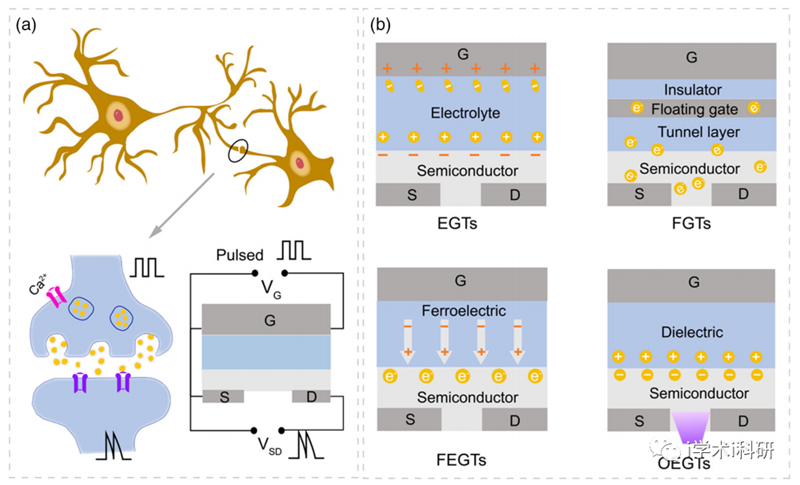
Figure 1. a) Analogy of artificial synapses and biological synapses. b) Schematic of different device configuration based on the unique operation principles.
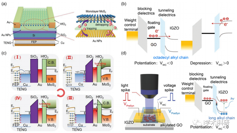
Figure 2. a) Schematic diagram of the mechanoplastic MoS2 synaptic transistor, trapped/de-trapped of electrons by Au nanoparticles (NPs) across HfO2tunneling layer. b) Band schematic of electron ejection (left) and electron injection (right) phases. c) Energy band Schematic under single displacement pulse stimulate of four stages to illustrate work mechanism. d) Operation mechanism of the sen-memory device at zero bias.
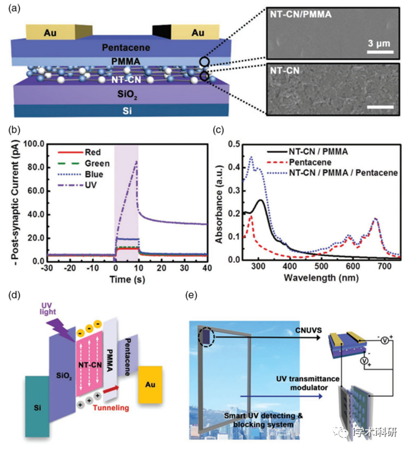
Figure 3. a) Schematic illustration of the C3N4-based UV-responsive synaptic transistors (CNUVS) structure and the scanning electron microscope (SEM) images of NT-CN and NT-CN/polymethyl methacrylate (PMMA) films. b) Graphs of ID as a function of time under R, G, B, or UV excited (VD ¼ 5 V, VG ¼ 0 V). c) UV–vis spectra of pentacene, NT-CN/PMMA, and NT-CN/PMMA/pentacene films. d) The energy-band illustration of the CNUVS measured by ultraviolet photoelectron spectroscopy. e) The smart system integrated by CNUVS and the UV transmittance modulator to detect and block UV.
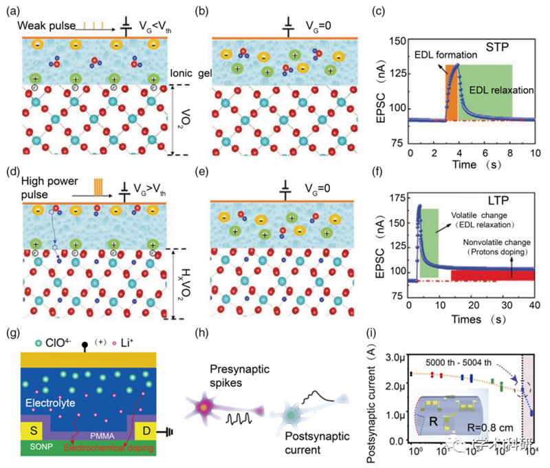
Figure 4. Brief schematic of the operation mechanism of electrolyte-gated synaptic transistor. a–c) The realized short-term potentiation (STP) behavior by modulating volatile electrostatic. d–f ) The realized long-term potentiation (LTP) behavior by modulating nonvolatile electrochemical reactions. g) Schematic diagram of electrochemical SnO2 nanoparticles (SONP)-based ion-storage and transfer characteristics of electrical processing synapse. h) Schematic of the synaptic information transmission with action potentials. i) The trend of postsynaptic current (PSC) with different bending times.
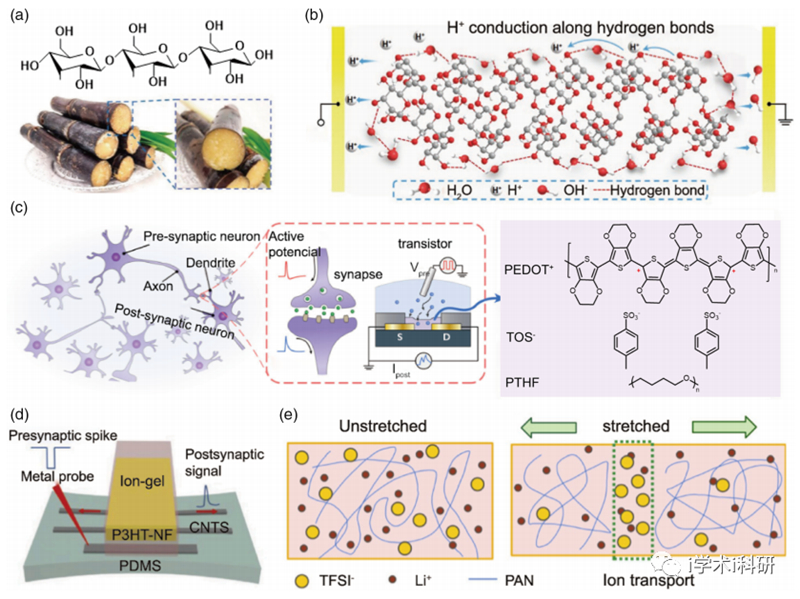
Figure 5. a) The material of the electrolyte layer dextran and the molecular structure. b) The process of proton migration along the hydrogen bonds connected by dextran molecule chains and water molecules. c) Schematic of organic electrochemical transistor (OECT) and synapse (left), the chemical structure diagram of tosylate (Tos), poly (3, 4-ethylenedioxythiophene) (PEDOTþ),and polytetrahydrofuran (PTHF) (right). d) Schematic of the device configuration of transistor. e) The schematic of the effect of stretching onion transport in ion-gel.
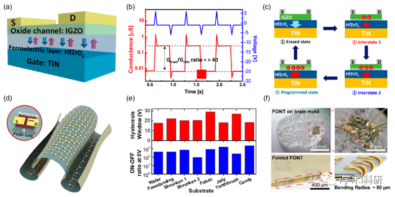
Figure 6. a) Device construction of ferroelectric synaptic transistor. b) Conductance was modulated by applying voltage pulses (from 6 V to 6 V)c) Schematic explaining the operation mechanism of data storage under pulse stimulation. d) Schematic device structure of the ferroelectric organic neuromorphic transistors (FONTs). e) The ON OFF ratios and hysteresis windows of devices attached to different substrates. f ) Photograph of the flexible FONTs attached to the PDMS brain mold and folded FONTs with a bending radius 50 μm.

Figure 7. a) Schematic diagram of tunable ferroelectric gate dielectric layer-based synaptic device. b) The device architecture of synaptic transistor. c) The working principle of AiS-TSO induced by tactile stimulation. d) Schematic of the synaptic operation mechanism of nanoscale channel organic ferroelectric synaptic transistor (NOFST).
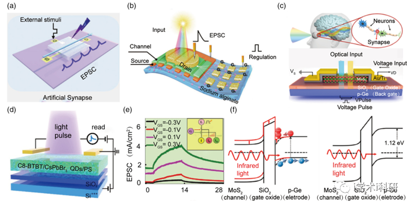
Figure 8. a) Schematic diagram of the artificial synaptic transistor. b) The device structure diagram of phototransistor network with sub-10 nm vertical coplanar-multiterminal. c) Schematic of the multilevel Ge-gated based optic-neural device structure. (The wavelengths of lasers light sources were 520 and 1550 nm.) d) Schematic of the phototransistor based on C8-BTBT/PS/ CsPbBr3 quantum dots (CPB QDs). e) The transformation process from STM to LTM triggered by VGS.
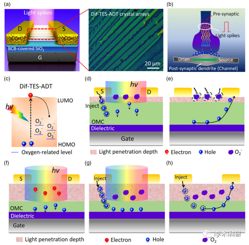
Figure 9. a) Schematic of the OMC array based photosynaptic transistor and cross-polarized optical micrograph of the Dif-TES-ADT crystal array. b) Schematic of the artificial photosynaptic device simulating the biological synapses. c) The charge transfer process from OMC to the oxygen-related level under light pulse to illustrate the working mechanism. d–e) Schematic diagram of the operating mechanisms for the photosynaptic trasistor with weak light. f–h) The operating mechanisms of the photosynaptic transistor under a strong light pulse.
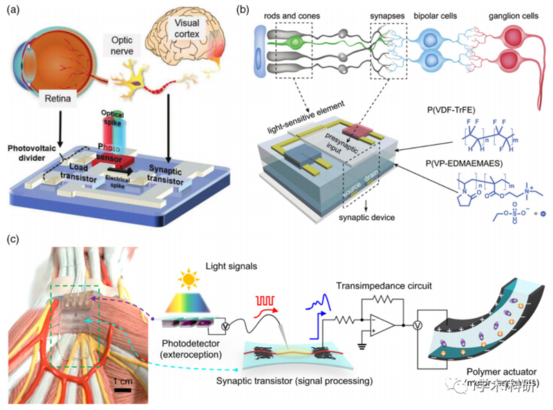
Figure 10. a) A optoelectronic neuromorphic system used to simulate the biological visual perception. b) Schematic diagram of a retina (the above). 3D structure diagram of a light-triggered organic neuromorphic device composed of a lightsensitive element and a synaptic device. c) Actual picture of a human structure model connected with optoelectronic synapses. In which,optoelectronic synaptic devices conclude with an artificial synapses and photodetector. Artificial synapses, trans-impedance circuit, and artificial muscle actuator formed a neuromuscular electronic system.
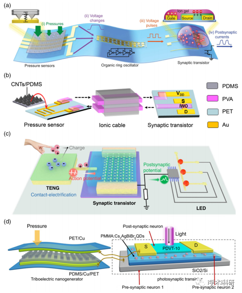
Figure 11. a) An artificial afferent nerve consists of an organic ring oscillator,a pressure sensor, and a synaptic transistor. b) The trend of PSC with bending times (radius of curvature: 0.8 cm). c) Schematic diagram of the graphene-based piezotronic artificial synapses. The schematic of the equivalent circuit through the coupling effect of piezoelectric potential using an ion gel.
总结与展望
在这篇评论中,作者系统地讨论了最先进的基于晶体管的人工突触的发展。讨论了材料的选择、载流子转移的机制和柔性器件的突触功能。这些人工突触装置的基本突触功能,如短期可塑性、长期可塑性和依赖尖峰时间的可塑性,都被很好地模拟出来。此外,还介绍了人工神经系统的最新发展,即结合突触晶体管和传感器来模拟视觉和触觉突触功能。总结了材料的选择、能量消耗和刺激信号等实现突触功能的基本要素。此外,还讨论了这四种类型的晶体管的优点和缺点。例如,浮动门突触晶体管表现出较大的开/关比率和可控的通道电导,用于非挥发性存储器。然而,由于基于电荷的记忆特性,需要一个大的工作电压。在低电压下工作的电解质门控突触器件具有较高的开关性能,而电解质的不稳定性,如离子液体,对器件性能有负面影响。铁电突触器件表现出较大的开/关比率和优良的多域结构,赋予了人工突触以逻辑功能和人工树突神经元。然而,切换铁电材料的极化状态所需的高工作电压是一个需要解决的难题。光电突触晶体管在人工视觉感知系统中具有带宽宽、能耗低、信号传输超快的优点。因此,进一步的研究应该集中在突触晶体管的这些局限性上,以实现优异的性能。
未来与材料设计、机制探索和应用相关的挑战和机遇依然存在。首先,有机半导体材料具有长期生物相容性、材料可调性、良好的机械灵活性和分子多样性等独特优势。然而,基于有机材料的突触装置的工作电压比基于无机材料的突触装置要高。其次,尽管人工突触系统取得了鼓舞人心的进展,但模拟复杂生物器官的人工感知系统的功能限制了几种简单的生物突触行为。为了满足复杂多样的要求,需要具有多种刺激的灵活的突触装置来处理多感官数据。因此,一个可能的解决方案是开发新型的、灵活的突触装置来实现多传感器的人工突触。此外,全面了解突触装置的载流子传输机制对于扩展突触的功能至关重要。第三,开发集成到基于晶体管阵列形式的人工突触装置是下一个研究前沿。因此,要实现阵列级的柔性突触系统,柔性突触器件的问题仍然存在,如可靠性、可扩展性和稳定性。基于柔性突触器件的下一代人工神经系统需要感觉部分和生物系统间信号的精确匹配。
文献链接Flexible Artificial Synapses Based on Field Effect Transistors: From Materials, Mechanics towards Applications, DOI: 10.1002/aisy.202200015https://doi.org/10.1002/aisy.202200015.
厦门柔性电子研究院
福建省协同创新院柔性电子产业技术分院
地址:厦门市集美区集美大道1995号科技成果转化加速器1期4F
邮编:361024 电话:0592-5366222 邮箱:admin@flex-elec.com
部分图片来源于网络,如有侵权请联系删除