
研究背景
在过去的二十年里,显示技术的不断发展显示出巨大的潜力,使人类的生活更加生动和舒适。显示技术已经从厚的电子管技术发展到薄的液晶(LC)策略和目前的柔性有机发光二极管(OLED)技术。与传统的刚性显示器相比,柔性显示器具有几个独特的特点,如重量轻、结构超薄、能耗低和高机械变形耐受能力。因此,它们已经获得了工业界和学术界的极大关注。例如,可折叠显示器可以忍受180°的大规模弯曲角度,弯曲半径低于5毫米甚至低于1毫米。然而,基于目前的减薄技术和铰链设计,已报道的基于OLED的柔性显示器和薄膜晶体管(TFT) 驱动的系统不能忍受<1毫米的弯曲半径和多维弯曲。它们主要受到显示器中现有部件的刚性和脆性的限制,如硅基TFT。
从技术上讲,实现柔性有不同的途径。(1) 物理弹性:任何极薄或直径极小的刚性材料都可以实现弹性。(2) 结构柔性:例如,导线连接的分形和弹簧配置可以为刚性芯片提供:宏观的柔性。(3)本质上的灵活性:设备中的材料(如聚合物和碳材料)具有柔性和可拉伸的性质。物理和结构灵活性的结合促进了折叠屏手机中铰链技术的发展。然而,这种手机的长期机械稳定性仍然是一个相当大的挑战。通常情况下,灵活性是由弯曲半径(R) 来量化的。R的减少导致材料的灵活性提高。与柔性和可拉伸设备不同,本征柔性显示器应同时满足三个关键要求:大的弹性变形、小的弯曲半径(<0.5 毫米)和高的拉伸应变(>25%),这决定了它们是否能随后被符合、折叠或滚动。有了这三个条件,本质上灵活的显示器可以改变对经常出现在我们生活中几乎所有方面的信息的看法。
研究成果
柔性电子产品的不断进步为人类生活带来了更多的便利和舒适。在这一领域,互连和新型显示应用被公认为是未来的重要方向。然而,由于显示面板的尺寸和形状有限,开发本征柔性显示是一个巨大的科学和技术挑战。为了解决这一难题,开发本征柔性电极材料、半导体材料和电介质材料,以及相关的柔性晶体管驱动器和显示面板至关重要。中国科学院化学研究所刘云圻院士联合郭云龙研究员以“Intrinsically flexible displays: key materials and devices”为题发表相关综述在National Science Review期刊上。在这篇综述中,主要从七个方面介绍这一领域的最新进展: 背景和概念、本征柔性电极材料、本征柔性有机半导体和用于有机薄膜晶体管(OTFT) 的介电材料、用于电致发光器件的本征柔性有机发光半导体,以及用于本征柔性显示器的OTFT驱动的电致发光器件。最后,对本征柔性显示器的未来发展提出了一些建议和展望。
图文导读
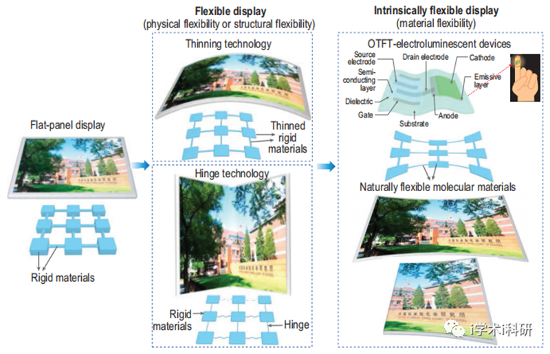
Figure 1. Schematic diagrams showing the development process of a display.
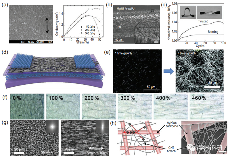
Figure 2. (a) Scanning electron microscopy (SEM) image of the SWCNT-polymer composite electrodes under 100% tensile strain (the arrow shows the stretching direction). (b) SEM image of the sheet crosssection for the rubber-like MWCNT forest/PU composites. (c) Normalized resistance (R/R0) of the MWCNT forest/PU composites as a function of repeated bending and twisting cycles. (d) Diagram showing the stretchable transistor using the multilayer graphene/graphene scrolls as electrodes under stretching. (e) SEM image of AgNWs prepared via the successive multistep growth method after one-time and seven-time growth, respectively. (f) Microscopic surface morphology of the stretchable, very long AgNW percolation network (VAgNPN) electrodes under stretching strain from 0% to 460%. (g) SEM images of the PEDOT: PSS/g-PDMS electrode film without (left) and with 100% (right) stretching strain. (h) Schematic representation (left) and SEM image (right) of the hierarchical multiscale AgNW/CNT hybrid nanocomposites.
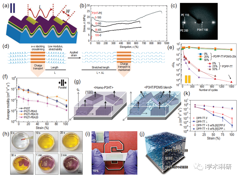
Figure 3. (a) Stretchable thin-film transistors fabricated on the topographic substrate with source/drain electrodes parallel to the topographic direction. (b) Stress-elongation profile of the deblock copolymer with different weight ratios of P3HT and polyethylene (PE). (c) The wide-angle X-ray diffraction patterns of a 35−65 P3HT-PE film under 600% stretching strain, which demonstrates a high degree of uniaxial or[1]der and crystallinity. (d) Visualization of the phase segregation concept. (e) The DC conductance of the neat PDPP-TT and PDPP-TT-PDMS polymer under 0∼50 tensile strain and multiple stretching cycles (0∼1500) parallel to the charge-transporting direction. (f) Average carrier mobility of the PII2T-PBA block polymers under stretching strain from 0% to 100% parallel to charge[1]transporting direction. (g) Schematic illustration of the distribution of P3HT NWs in homo-P3HT (left) and P3HT NW/PDMS blend films (right) on Si wafer. (h) Fabrication process of the P3HT nanofilm on the water surface. (i) Three-dimensional (3D) schematic illustrating the dispersion of poly(2,5-bis(2-octyldodecyl)-3,6-di(thiophen2-yl)diketopyrrolo[3,4-c]pyrrole-1,4-dione-alt-thieno[3,2-b]thiophen) (DPPT-TT) polymer in the SEBS matrix for the CONPHINE film. (j) Morphology of the CONPHINE film on a PDMS substrate under 0% and 100% stretching strains. (k) Mobility of fully stretchable transistors with neat DPP-TT and DPP-TT/5 wt% CPP blends as the semiconducting materials, under 0%tion.
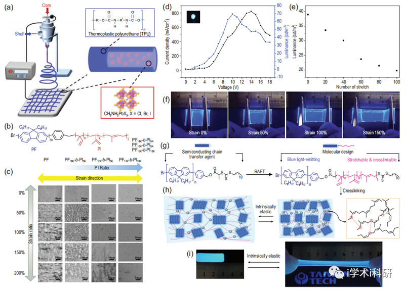
Figure 4. (a) Schematic of the coaxial electrospinning core-shell polyurethane (TPU)/perovskite luminous nanofibers. (b) Molecular structure of the PF-b-PI rod-coil block copolymer with different rod/coil ratio configurations. (c) Photographic images of the copolymer films under a strain of 0%, 50%, 100%, 150% and 200%. (d) I−V−L characteristic curves of the stretchable PF12K-b-PI5K LEDs. (e) Luminance-stretching cycle characteristics of a device under different cycles at a constant strain of 20%. (f) Photographic images of the PF12K-b-PI5K LEDs under ultraviolet light and a strain of 0%, 50%, 100% and 150%. (g) Molecular structure of the stretchable PF-b-PI copolymer. (h) Schematic illustration of the deformable polymer with a PF-b-PI1.8 matrix and cross-linker 1, 9-nonanedithiol (DT). (i) Photographic images of the cross-linked stretchable PF-b-PI1.8 film at a strain of 0% and 300%.
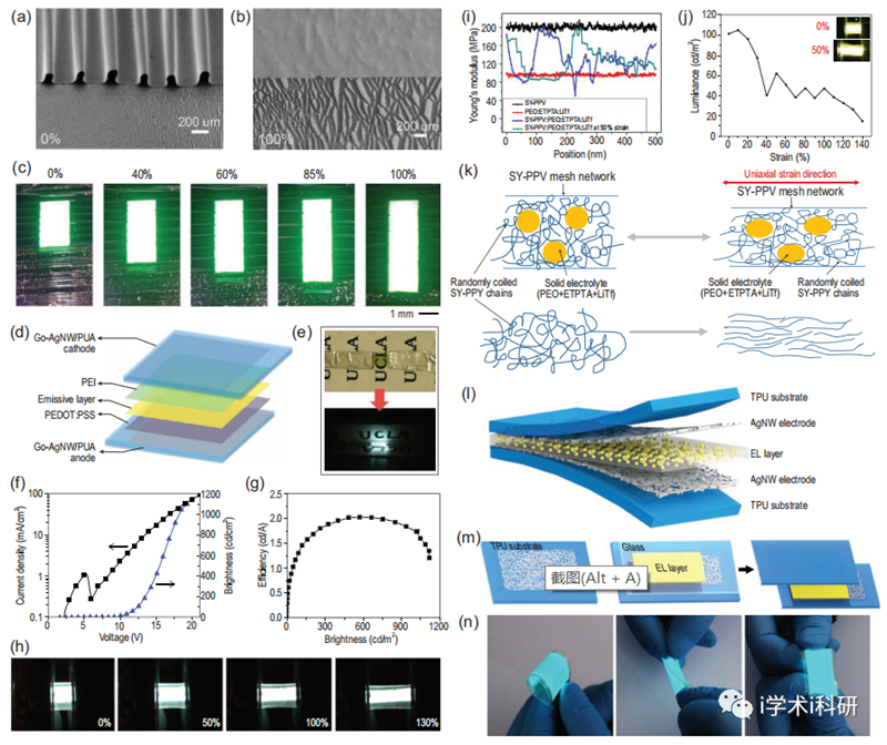
Figure 5. SEM images of the stretchable OLEDs at (a) 0% strain and (b) 100% strain. (c) Photographic images of the stretchable OLEDs at varying strain values from 0% to 100%. (d) Device structure of the fully stretchable OLED using GO-AgNWs/PUA composite electrode as counter electrodes. (e) Photographic images of a semi-transparent unlit stretchable PLED (top) and a stretchable PLED illuminated at a voltage of 13 V (bottom). (f) Current-voltage curve and (g) luminescence-current efficiency curve of the stretchable PLED. (h) Photographic images of a stretchable PLED at different strains (initial emissive area of 3 mm × 4 mm with a driven voltage of 14 V). (i) Cross-sectional Young’s modulus curves of different samples obtained from peak force quantitative nanomechanical mapping. The mixture of SY-PPV and polymer electrolyte forms an effective nano-interpenetrating network to achieve tensile properties. (j) Brightness-strain characteristic curve of polymer light-emitting electrochemical cell (PLEC). (k) Schematic of the nano-interpenetrating networks under different strains. The solid electrolyte dissipates the external stress, thereby preserving the general phase morphology of SY-PPV. (l) Structure of the alternating current electroluminescent (ACEL)device. (m) Fabrication route of the ACEL device. (n) Photographic images of the ACEL device powered by a commercial electroluminescence (EL) driver under bent, twisted and stretched states.
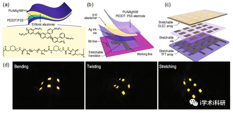
Figure 6. (a) Device structure of the stretchable light-emitting electrochemical cell, where the molecular structures of su[1]per yellow and stretchable ion-conducting polymer are highlighted. (b) 3D structural layout of a single active-matrix organic light-emitting electrochemical cell (AMOLEC) pixel. (c) 3D layout scheme of the vertical integrated active matrix and PLEC array. (d)Photographic images of the AMOLEC skin display pixels subjected to bending, twisting and stretching.
总结与展望
基于OSC和OTFT的优势,基于OTFT的显示器有望成为本征柔性显示器的基本单元。尽管在本征柔性材料和技术方面已经取得了重大突破,但在本征柔性显示器的实际实现方面仍有许多问题没有得到解决。
如何创建具有高载流子迁移率的内在柔性OSC是人们关注的主要焦点。混合弹性体和共轭聚合物是制备可拉伸聚合物半导体的一种常见策略。然而,只有基于P3HT和DPP的共轭聚合物在可拉伸聚合物半导体中得到利用。N型和双极可拉伸聚合物半导体还从未被创造出来。混合机制以及表面能和分子量等条件都需要得到澄清。同时,关于本征柔性OSC (包括传输材料和发光材料)的结构-应变-电光性能的统一结构-性能关系的研究仍处于起步阶段,需要对材料的可拉伸电光性能进行进-步的调查和新的设计理念。
基板材料可直接影响本征柔性显示器的弯曲半径。它们的选择在很大程度上取决于电介质材料和设备的制造程序。介质材料和基底材料之间的弹性模量差异很容易诱发泊松效应,并在多次拉伸-释放循环中造成薄弱的界面接触。因此,必须确保电介质层和衬底的应力松弛和表面能量相似。此外,大多数报道的可拉伸电极,如CNTs和AgNWs,具有较高的表面粗糙度,这对电极和活性层之间的界面接触是不利的。与弹性粘合剂的混合和构建层-异质结电极是克服这一问题的有希望的策略。
OTFT驱动的电致发光器件的性能可以通过形态调节(结晶状态、取向)和界面改进来提高。因此,溶液加工技术和界面工程的发展是改善光电性能的原因。然而,多级尺度的高分辨率图案仍是研究重点和挑战。此外,多种功能器件的集成往往需要合理的电路设计和全面的性能测量。许多问题需要解决,如功能层之间的滑移、器件的一致性、稳定性和可重复性。总的来说,机遇和挑战并存,坚信在学术界和工业界的合作努力下,可以取得重大突破。在不久的将来,本质上灵活的显示器将大大改变我们的生活方式。
文献链接:Intrinsically flexible displays: key materials and devices, National Science Review 9: nwac090, 2022, https://doi.org/10.1093/nsr/nwac090
厦门柔性电子研究院
福建省协同创新院柔性电子产业技术分院
地址:厦门市集美区集美大道1995号科技成果转化加速器1期4F
邮编:361024 电话:0592-5366222 邮箱:admin@flex-elec.com
部分图片来源于网络,如有侵权请联系删除